
The performance advantages of silicon carbide, a third-generation semiconductor manufacturing materi
The third-generation semiconductor manufacturing material silicon carbide has outstanding performance advantages.

3C\4H\6H-SiC structure diagram
The first-generation semiconductor materials mainly refer to elemental semiconductor materials represented by silicon (Si) and germanium (Ge), which are widely used, including integrated circuits, electronic information network engineering, computers, mobile phones, etc. Among them, the most typical application is integrated circuits, mainly used in low-voltage, low-frequency, and low-power transistors and detectors. Silicon-based semiconductor materials are currently the semiconductor materials with the largest output and the widest application, with more than 90% of semiconductor products being made from silicon-based materials. However, the physical properties of silicon limit its application in optoelectronic and high-frequency electronic devices. For example, its indirect bandgap characteristic determines that it cannot achieve high electro-optical conversion efficiency; moreover, its bandgap width is relatively narrow, and the saturated electron mobility is low, which is not conducive to the development of high-frequency and high-power electronic devices. Silicon-based devices reach their performance limits in high-voltage scenarios above 600V and high-power applications.
The second-generation semiconductor materials mainly refer to compound materials represented by gallium arsenide (GaAs) and indium phosphide (InP). Currently, the key communication chips used in mobile phones are made from similar materials. The electron mobility of gallium arsenide is about six times that of silicon, and it has a direct bandgap. Therefore, its devices have high-frequency and high-speed optoelectronic performance compared to silicon-based devices, making it widely used in the fields of optoelectronics and microelectronics. It is a key substrate material for manufacturing semiconductor light-emitting diodes and communication devices. Due to the insufficient bandgap width and low breakdown electric field of second-generation semiconductor materials, their application in high-temperature, high-frequency, and high-power devices is limited. In addition, the toxicity of gallium arsenide may cause environmental pollution issues and pose a potential threat to human health.
The third-generation semiconductor materials refer to wide bandgap semiconductor materials represented by silicon carbide (SiC), gallium nitride (GaN), zinc oxide (ZnO), diamond, and aluminum nitride (AlN). They are mostly used in scenarios such as communications, new energy vehicles, high-speed railways, satellite communications, and aerospace. Among them, the research and development of silicon carbide and gallium nitride are relatively mature. Compared with the first two generations of semiconductor materials, third-generation semiconductor materials have a large bandgap width and advantages such as high breakdown electric field, high thermal conductivity, high electron saturation rate, and strong radiation resistance. Therefore, semiconductor devices made from third-generation semiconductor materials can not only operate stably at higher temperatures and are suitable for high-voltage and high-frequency scenarios, but can also achieve higher operational capability with lower electrical energy consumption.
Silicon carbide is aⅣ-Ⅳ group compound semiconductor material composed of carbon and silicon. It has multiple allotropic types and is the third hardest substance in the world, being very stable in terms of thermal, chemical, and mechanical properties. In terms of physical properties, SiC has the characteristics of high hardness, high wear resistance, high thermal conductivity, high thermal stability, and good heat dissipation. In terms of chemical properties, the surface of SiC easily forms a silicon oxide film to prevent further oxidation, but this oxide film will rapidly undergo oxidation reactions at high temperatures.
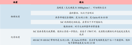
Summary of the physical and chemical properties of silicon carbide
The typical structures of silicon carbide can be divided into two categories. One is the cubic silicon carbide crystal form with a zinc blende structure, called3CSiC orβ-SiC, where 3 refers to the number of planes in the periodic stacking order. The other is a large-period structure with a hexagonal or rhombohedral structure, among which typical ones include 6H-SiC, 4H-SiC, 15R-SiC, etc., collectively referred to as α-SiC. Among them, 4H-SiC and 6H-SiC are two materials required for semiconductors. Silicon carbide has similar characteristics to other semiconductor materials. The saturated electron velocity of 4H-SiC is twice that of Si, thus providing SiC components with higher current density and higher voltage, and it is often used as a material for silicon carbide power devices. The biggest difference between 6H-SiC and 4H-SiC is that the electron mobility of 4H-SiC is twice that of 6H-SiC, because 4H-SiC has a higher horizontal axis mobility. During the growth process of silicon carbide crystals, parameters such as the silicon-to-carbon ratio, growth temperature gradient, crystal growth rate, and gas flow and pressure need to be precisely controlled; otherwise, polytype inclusions are easily generated, resulting in unqualified crystals..